 Fall 2017
 Project 7: CPU
Due 14 November 2017
The purpose of this project is to build a simple CPU that integrates all the necessary aspects of a general-purpose computer. This is a two-week project. You will need to demonstrate your functional alu with the alu test program during the labs on November 6-7.
Tasks
The overall task is to create a functional CPU, using a ROM for the program memory, a RAM for the data memory, and a separate ALU circuit.
Examine the CPU Design before starting.
- Make a new project for lab 7 in a new folder. I'll refer to the project and top-level circuit as cpu.
- Using the Tools:MegaWizard Plugin Manager, create a 1-port ROM that has 256 words of 16 bits each. I'll refer to this circuit as ProgramROM. Tell it to initialize the ROM using this MIF file. This step will create a VHDL file that you need to add to your project.
- Using the Tools:MegaWizard Plug0in Manager, create a 1-port RAM that has 256 words of 16 bits each. I'll refer to this circuit as DataRAM, Tell it to initialize the RAM using this MIF file. This step will create a VHDL file that you need to add to your project.
-
Create a top-level VHDL file called cpu.vhd with an entity called cpu.
Your cpu entity should have a clock (std_logic), reset (std_logic),
input port (std_logic_vector(7 downto 0)), and an output port
(std_logic_vector(15 downto 0)). You can use the 4-state Moore
machine template, if you wish.
To use the cpu test bench for simulation, you will also need to add the following signals to your cpu port statement. The port statement that matches the cpubench usage is below.
  port (
    clk   : in  std_logic;                       -- main clock
    reset : in  std_logic;                       -- reset button

    PCview : out std_logic_vector( 7 downto 0);  -- debugging outputs
    IRview : out std_logic_vector(15 downto 0);
    RAview : out std_logic_vector(15 downto 0);
    RBview : out std_logic_vector(15 downto 0);
    RCview : out std_logic_vector(15 downto 0);
    RDview : out std_logic_vector(15 downto 0);
    REview : out std_logic_vector(15 downto 0);

    iport : in  std_logic_vector(7 downto 0);    -- input port
    oport : out std_logic_vector(15 downto 0));  -- output port
Don't forget to assign the various signals to their matching outputs. The PC should be assigned to PCView, the IR should be assigned to the IRview, and so on. You will also need to be sure to assign your internal output register (OUTREG) signal to oport.
Create component statements for both the ProgramROM and DataRAM in the architecture header.
-
Create an arithmetic logic unit VHDL design file, alu.vhd. Add the
file to your project. You can use this template
as the basis for the ALU circuit design. The circuit is completely
asynchronous, and it does not require any additioanl signals beyond
what is in the template in order to build the circuit.
There are four condition bits that need to be set, based on the ALU operation.
- Zero: cr(0) should be set to '1' if the ALU operation resulted in a zero value, bits 15 downto 0 of the result.
- Arithmetic overflow: cr(1) should be set to '1' if an addition or subtraction operation resulted in an overflow. 2's complement overflow occurs when the two operands are the same sign and the result is a different sign.
- Negative: cr(2) should be set to '1' if the sign bit of the result is '1' (negative).
- Carry out: cr(3) should be set to '1' if a '1' was shifted out of the left or right side of the input, or if an arithmetic operation resulted in a carry.
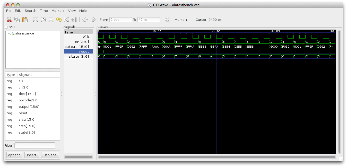
When you have your alu design complete, test it using this testbench program. It should produce the output below using ghdl/gtkwave.
ghdl -a alutestbench.vhd alu.vhd
ghdl -e alutestbench
ghdl -r alutestbench --vcd=alutestbench.vcd
gtkwave alutestbench.vcd
-
As noted in the CPU design, you probably
want to use a 9-state state machine for your CPU. The first state is
a startup state, and the final state is a halt state. After eight
clock cycles, this state should move to the fetch state. You will need
a small internal counter (3 bits) to implement the pause in the start
state. The state machine should never return to the start state unless
it is reset.
The remaining states are fetch, execute-setup, execute-process, and execute-write. Set up your overall state machine structure to follow this model. Each state always leads to the next state in the process, with the execute-write state going back to the fetch state.
Set up your skeleton nine state state machine, putting in only the state transitions for now. No state should go to the halt state (yet).
-
Create the remaining internal signals you need for your CPU. There
are a lot. Following the cpu diagram,
there should be a signal for every register, including the condition
register. In addition, you will need a signal to represent the two
ALU input buses and the ALU output bus.
You will also want signals for the output port register (OUTREG), the ROM data-out wire, the RAM data-out wire, the RAM write-enable wire, the ALU opcode, and the ALU condition argument.
-
Port map your ProgramROM, DataRAM, and ALU circuits into your cpu.
The clock, PC and ROM data wire should map to the ROM clock, address,
and output.
The MAR and MBR should map to the RAM address and data-in parameters. The RAM data wire, RAM write enable wire, and clock should map to the RAM output, RAM write enable (wren) and clock.
The srcA, srcB, and dest parameters should map to the ALU input buses and the output bus, respectively. Map the ALU opcode and condition outputs to their respective signals.
-
Implement your CPU.
- If the reset button is activated, set the registers PC, IR, OUTREG, MAR, MBR, RA, RB, RC, RD, RE, SP, and CR to zeros. The state should be reset to the startup state and the small counter should be reset to zeros.
- The startup state should increment the small counter and stay there until it reaches 7. Then it should move to the fetch state.
- The fetch state should copy the ROM data wire contents to the IR, increment the PC, and move to the execute-setup state.
-
The execute-setup state should set up each of the instructions.
- For the load and store instructions, move the correct RAM address into the MAR. If IR(11) is set, use the 8 low bits of the IR plus register E (RE). If IR(11) is not set, just use the low bits of the IR. You will also need to put the data to write into the RAM into the MBR.
- For the unconditional branch, set the PC to the low 8 bits of the IR.
- For the conditional branch, check the condition flag specified in the instruction and move the low 8 bits of the IR to the PC if the condition is true.
- For the CALL instruction, set the PC to the low 8 bits of the IR, set the MAR to the SP, set the MBR to the concatenation of four zeros, the CR, and the PC. Then increment the stack pointer.
- For the RETURN instruction, set the MAR to the SP and decrement the SP.
- For the push operation, put the current vaue of the SP into the MAR, increment the SP, and put the value specified in the source bits into the MBR.
- For the pop operation, put the value (SP-1) into the MAR and decrement the SP.
- For the binary ALU operations (add, sub, and, or xor) set up srcA and srcB.
- For the unary ALU operations (shift, rotate) set up srcA and put the direction bit in the low bit of srcB.
- For the move operation, set up srcA, which will come either from a register or be a sign extended value from the immediate value bits of the IR (bits 10 downto 3).
- The execute-process state should set the RAM write enable signal to high if the operation is a store (opcode 0001, or integer 1), a push, or a CALL.
- The execute-wait state should do nothing. All instructions can pass through this state, but it is required only for instructions that are accessing the RAM (POP, LOAD, and RETURN).
-
The execute-write state should handle the final stage of the various
operations. At the beginning of the state, it should set the write
enable flag to '0'.
- For the load operation, it should write the contents of the RAM data wire to the specified destination register.
- The store, unconditional branch, conditional branch, call, and push operations require no action.
- The return operation requires that the proper parts of the RAM data wire be written to the PC and CR.
- For the pop operation, it should write the value of the RAM data wire to the destination specified in the instruction.
- For the write to the output port, it should set the output port register OUTREG to the specified value.
- For the load from the input port, it should write the input port value to the specified register.
- For the binary and unary arithmetic operations (add, sub, and, or, xor, shift, rotate), it should write the destination value to the proper register. It should also assign the ALU condition flags to the condition register [CR].
- For the move operation it should write the destination value to the proper register and set the condition register [CR] from the ALU condition flags.
- The execute-return-pause states, there are two of them, are required for RETURN instructions so that the next instruction can be accessed from the program ROM before heading back to the fetch state. On the RETURN instruction needs to use these two states.
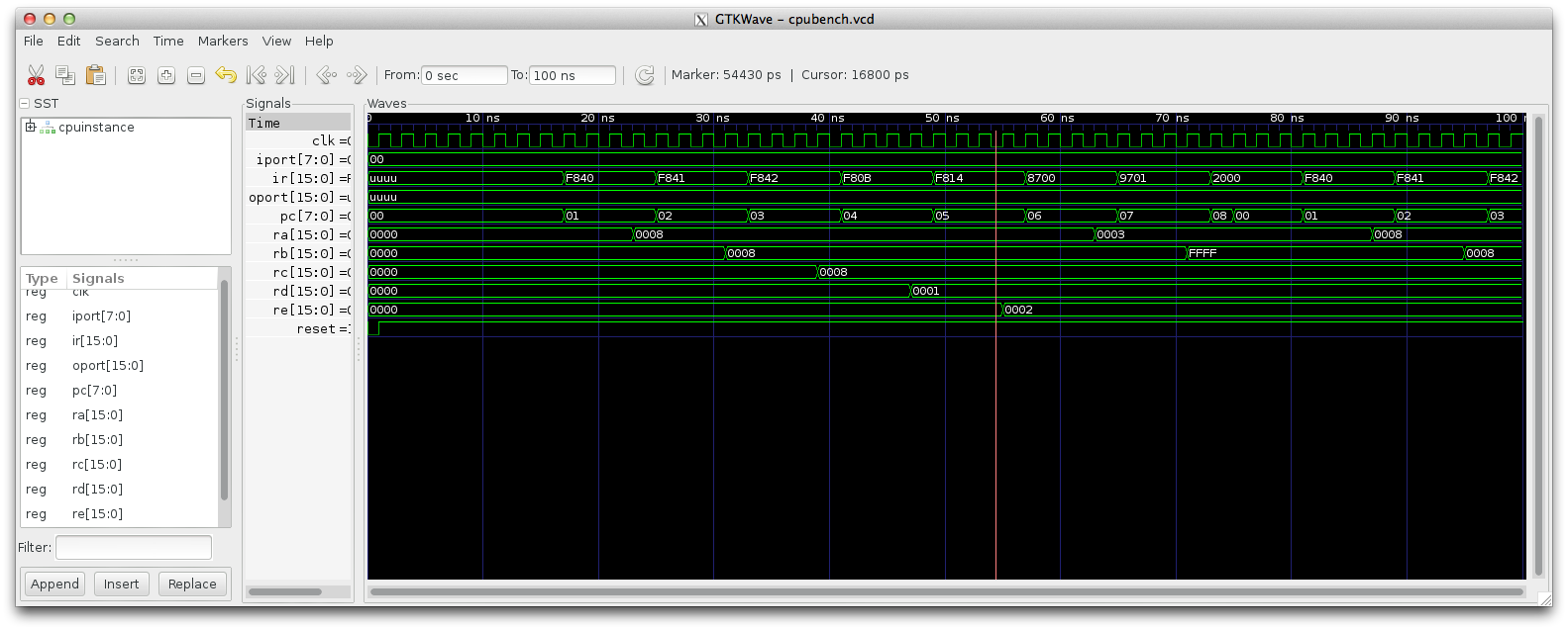
Test your CPU using the program given in the programROM.mif file above and using the cpubench.vhd test file. You should get a simulation like the following. Note that on the second command below you need to make sure the filenames match your own.
ghdl -a --ieee=synopsys -fexplicit --work=altera_mf /opt/altera/12.1/quartus/eda/sim_lib/altera*.vhd
ghdl -a --ieee=synopsys --work=altera_mf cpubench.vhd cpu.vhd alu.vhd programROM.vhd dataRAM.vhd
ghdl -e --ieee=synopsys -fexplicit --work=altera_mf cpubench
ghdl -r cpubench --vcd=cpubench.vcd
gtkwave cpubench.vcd &
-
Here are some more test programs you can try out. Read the .mif files
to understand whey they are doing and what you should expect for outputs.
- testpush.mif an MIF file for testing push and pop.
- testcallmif an MIF file for testing a function call.
- Write a program for your computer that creates the first 10 values of the fibonnaci sequence. Try to do it with a for loop. Simulate your circuit and demonstrate that it works.
Extensions
- Download your CPU to the board and demonstrate it works properly. No credit for this extension unless you somehow document it working as part of your report.
- Write more programs, such as an unsigned multiply program or a program that includes functions (CALL/RETURN). This is the best extension. Get yourself used to writing programs on this CPU.
- Write the fibonnaci sequence program using recursion.
- Write a program using something like Python that can generate an MIF file from some other, more easily readable, format.
- Be creative with the use of the input signal.
Writeup
Create a wiki page with your writeup. For each task, write a short description of the task, in your own words.
- Include a description of your top-level design.
- Include the initial contents of both your RAM and ROM.
- Include the screen shot of your simulation.
- Describe the hardware testing you undertook to prove the circuit works.
- Include a description, and pictures, of any extensions.
Handin
Give your wiki page the label cs232s17project7.
Put your VHDL files in zip file in your private subdirectory on the courses server. Please put just the vhdl and mif files on the server.