 Fall 2019
 Project 5: Programmable Lights II
The purpose of this project is to build a more sophisticated programmable light display. The machine language for this project includes both a conditional and an unconditional branch, enabling you to implement loops in your program.
Programmable Circuit Design
The new programmable light display will be a state machine with three states that can execute four types of instructions. Each instruction will be 10 bits long. The state machine has two data registers, the light register [LR] and the accumulator [ACC], both of which hold 8-bits. The instruction set is given below.
| Opcode | Format | Description |
|---|---|---|
| 00 | [C1 C0] [Dest1 Dest0] [Src1 Src0] [Val3 Val2 Val1 Val0] | Move from SRC to DEST |
| Dest10: 00 = ACC, 01 = LR, 10 = ACC low 4 bits, 11 = ACC high 4 bits | ||
| Src10: 00 = ACC, 01 = LR, 10 = IR low 4 bits sign extended, 11 = all 1s | ||
| 01 | [C1 C0] [Op2 Op1 Op0] [Src1 Src0] [Dest0] [Val1 Val0] | Binary operator DEST = DEST op SRC |
| Op210: 000 = add, 001 = sub, 010 = shift left, 011 = shift right maintain sign bit | ||
| Op210: 100 = xor, 101 = and, 110 = rotate left, 111 = rotate right | ||
| Src10: 00 = ACC, 01 = LR, 10 = IR low 2 bits sign extended, 11 = all 1s | ||
| Dest0: 0 = ACC, 1 = LR | ||
| 10 | [C1 C0] [U3 U2 U1 U0] [Addr3 Addr2 Addr1 Addr0] | Branch to ADDR |
| 11 | [C1 C0] [Src0] [U2 U1 U0] [Addr3 Addr2 Addr1 Addr0] | Branch to ADDR if SRC is 0 |
| Src0: 0 = ACC, 1 = LR |
There are four types of instructions: MOVE (00), BINARY (01), BRANCH (10), CONDITIONAL BRANCH (11). Move instructions copy data from the source location to the destination. Binary instructions execute some type of binary operation on two source values and store the result in the destination. In this instruction set, the destination is also one of the source values. Branch instructions uncondtionally branch to the address given in the instruction. Conditional branch instructions go to the address in the instruction only if the source register is equal to zero.
Tasks
- Setup
Start by creating a project in Quartus. I'll refer to the project as pld2 for the top level entity.
- Create a ROM to hold the program
Create a simple read-only memory [ROM] using VHDL. You can use last week's ROM as a starting point. Call it pldrom.
The pldrom should take one input signal addr that should be a 4-bit std_logic_vector. It should have one output signal data that should be a 10-bit std_logic_vector.
The content of your ROM architecture should be a single conditional signal assignment. You can use the following for testing. Later, you will need to write your own program. The 10-bit values stored at each address location are the program.
data <= "0001100000" when addr = "0000" else -- move 0s to LR 00000000/00000000 "0001110000" when addr = "0001" else -- move 1s to LR 11111111/00000000 "0001101010" when addr = "0010" else -- move 1010 to LR 11111010/00000000 "0010101000" when addr = "0011" else -- move 8 to ACC 11111010/00001000 "0101001100" when addr = "0100" else -- shift LR left "0100011000" when addr = "0101" else -- add -1 to ACC "1100001000" when addr = "0110" else -- branch if zero "1000000100" when addr = "0111" else -- branch "0001110000" when addr = "1000" else -- set LR to 1s 11111111/00000000 "1000000000" when addr = "1001" else -- branch to zero 11111111/00000000 "0101010101" when addr = "1010" else -- garbage "1010101010" when addr = "1011" else -- garbage "1100110011" when addr = "1100" else -- garbage "0011001100" when addr = "1101" else -- garbage "0000000000" when addr = "1110" else -- garbage "1111111111"; -- garbage - Start the main design
Make a new VHDL file. Name the entity pld2. You can use your VHDL code from the prior project as a starting point, if you wish (but you can also start over from scratch). Make the following quick modifications. (Leave the slowclock process.)
- Update the IR, ROMvalue, and pldrom component statement to use 10 bits for the instructions.
- The state_type will need three states: sFetch, sExecute1, and sExecute2.
- Add two new internal signals ACC and SRC that are 8 bit UNSIGNED type.
- Update the reset case so you are assigning 10 bits to the IR.
- Update the sFetch case so the next state is sExecute1.
- Delete all of the current code under state sExecute. Then set up cases for when sExecute1 and when sExecute2.
- Define the Execute 1 actions
In state sExecute1, the move and binary operation instructions should assign the appropriate value to the SRC signal. The move instruction uses IR(5 downto 4) and the binary instruction uses IR(4 downto 3).
The two branch instructions should assign the appropriate value to the PC. In the case of the conditional branch, it should assign a new address to the PC only if the specified register (ACC or LR) is equal to 0.
- Define the Execute 2 actions
In state sExecute2 the move instruction should assign the correct bits of SRC to the correct destination as specified by IR(7 downto 6).
The binary instruction should assign to either the ACC or LR--depending upon IR(2)--the result of the specified binary operation as given in IR(7 downto 5).
The two branch instructions should do nothing in execute 2.
- Test the circuit
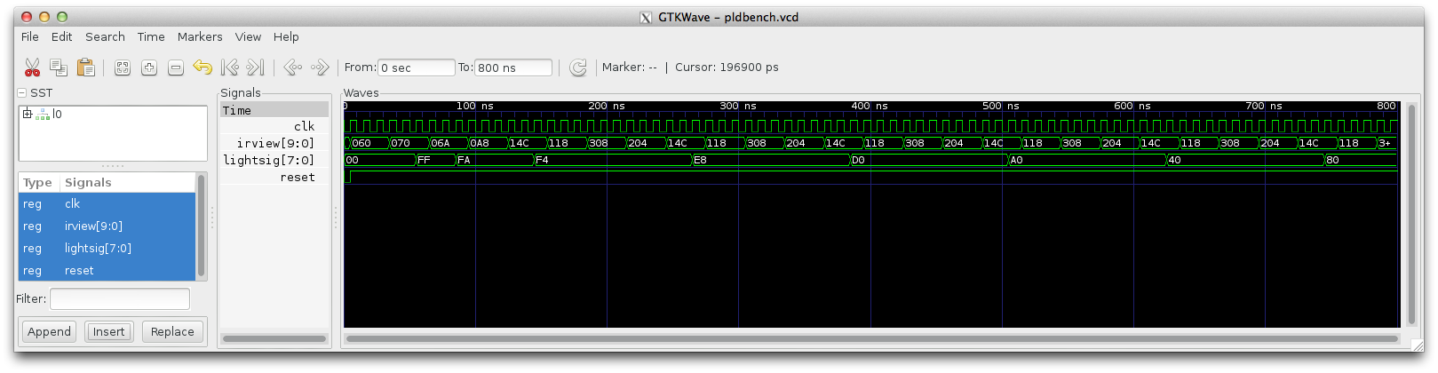
Test your system using this test bench file. If you still are using a slowclock signal, assign slowclock <= clk; for the simulation. Then set it back when testing on the board. If you run the program listed above, you should get the output below. Note that you may need to rename the circuit in the pldbench.vhd file to match your top level entity. (Click on the image to make it bigger.)
ghdl -a pldbench.vhd pld.vhd pldrom.vhd
ghdl -e pldbench
ghdl -r pldbench --vcd=pldbench.vcd
gtkwave pldbench.vcd &
- Write a specific program
Write a program that loads 16 into the light register and has it count down to 0. Then it should flash between all 1s and all 0s 8 times and repeat from the beginning.
- Write two more programs
Write two more programs. You should make use of branching in at least one of your programs. Be prepared to demonstrate your favorite at the beginning of lab.
Extensions
- Make longer programs (make the ROM bigger).
- Write more programs.
- Write a simple assembler (in python, for example) that converts instructions from a simple, human readable language, into the set of machine instructions for your pldrom.
- Add a hold/freeze button to the display.
- Add one or more switches/buttons that let you speed up or slow down the clock.
- Add instructions to the instruction set. You can add variations on the branch instuctions without adding more bits to the instruction length by making use of their unused bits. For example, you could add branch conditions like > 0, < 0 or make comparisons between the values in the two registers.
- Be creative.
Report
Create a wiki page with your report. For each task, write a short description of the task, in your own words.
- Include a description of your top-level design.
- Include a description of the three programs you wrote. The report can contain either a detailed explanation or you can put a detailed explanation in your VHDL code and a qualitative explanation in the report.
- Include a waveform simulation (gtkwave output) of the required program.
- Include either a waveform simulation or a video of your two additional creative programs.
- Describe any other testing you undertook to prove the circuit works.
- Include a description, and pictures, of any extensions.
Handin
Give your wiki page the label cs232f19project5.
Put your VHDL files in a folder called project5 in your private subdirectory on the courses server. Be sure your code is properly commented, including having your name at the top of each code file.