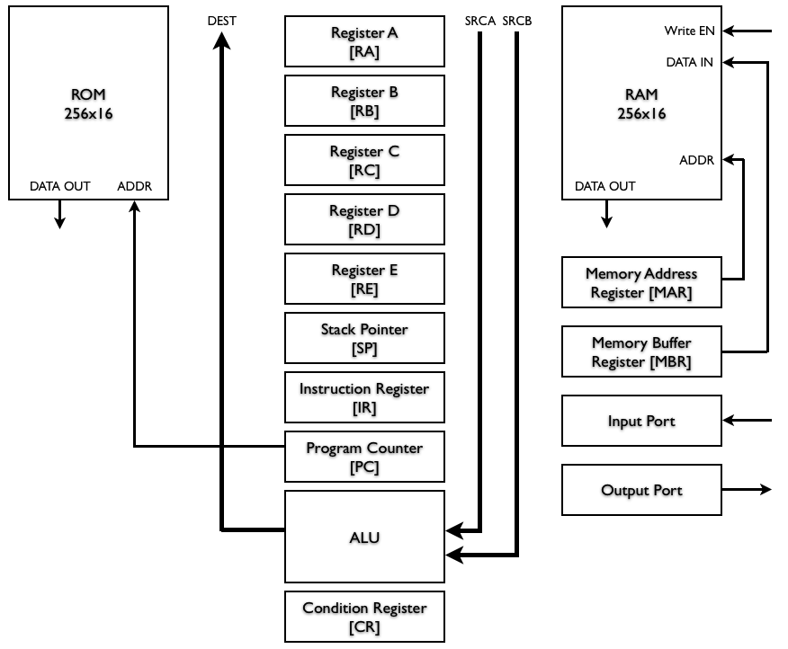
The register layout is shown in the graphic above. The instruction set is given below. It is modeled on the PowerPC RISC architecture, although the size and number of working registers is significantly reduced.
Registers A-E, the Stack Pointer, the MBR, and the Instruction Register are all 16 bit registers. The MAR needs to have enough bits to address all of memory (8 bits). The input and output ports can be 8-bits (if you don't want to assign lots of pins). The program counter is 8-bits, and the Condition Register is 4-bits. The ALU circuit takes in two 16-bit values and an opcode and outputs the 16-bit result as well as the 4-bits for the Condition Register.
The instructions are 16 bits. All instructions have a 4-bit opcode in bits (15 downto 12), with some instructions having an additional one or two bits of opcode. The remaining bits are used to specify source and destination registers, addresses, or immediate values. Instructions that have an address make use of the low 8 bits of the instruction to hold the information.
| Instruction | opcode | Remaining bits |
|---|---|---|
| Load from RAM | 0000 | R-DDD-AAAAAAAA: DDD = dest (table B), R = add register E to immediate value, AAAAAAAA - immediate address value |
| Store to RAM | 0001 | R-SSS-AAAAAAAA: SSS = src (table B), R = add register E to immediate value, AAAAAAAA - immediate address value |
| Unconditional Branch | 0010 | UUUU-AAAAAAAA: U = unused, AAAAAAAA = immediate address value. |
| Conditional Branch | 0011 | 00-CC-AAAAAAAA: CC = condition (00 = zero, 01 = overflow, 10 = negative, 11 = carry), U = unused, AAAAAAAA = immediate address value. |
| Call | 0011 | 01-UU-AAAAAAAA: the cpu should push the PC and CR on the stack and then jump to the immediate address value AAAAAAAA. |
| Return | 0011 | 10-UU-UUUUUUUU: the cpu should pop the CR and then pop the PC to continue execution at the stored address. |
| Exit | 0011 | 11-UU-UUUUUUUU: The CPU should enter a halt state and not leave until the user resets the circuit. |
| Push | 0100 | SSS-UUUUUUUUU: SSS = src (table C) U = unused, operation puts the value into memory at location SP and increments SP. |
| Pop | 0101 | SSS-UUUUUUUUU: SSS = dest (table C) U = unused, operation reads the value from memory at location SP-1 and decrements SP. |
| Store to Output | 0110 | SSS-UUUUUUUUU: SSS = dest (table D) U = unused. |
| Load from Input | 0111 | SSS-UUUUUUUUU: SSS = dest (table B) U = unused. |
| Add | 1000 | SSS-TTT-UUU-DDD: SSS = srcA (table E), DDD = dest (table B), TTT = srcB (table E) |
| Subtract | 1001 | SSS-TTT-UUU-DDD: SSS = srcA (table E), DDD = dest (table B), TTT = srcB (table E) |
| And | 1010 | SSS-TTT-UUU-DDD: SSS = srcA (table E), DDD = dest (table B), TTT = srcB (table E) |
| Or | 1011 | SSS-TTT-UUU-DDD: SSS = srcA (table E), DDD = dest (table B), TTT = srcB (table E) |
| Exclusive-or | 1100 | SSS-TTT-UUU-DDD: SSS = srcA (table E), DDD = dest (table B), TTT = srcB (table E) |
| Shift | 1101 | R-SSS-UUUUU-DDD: SSS = srcA (table E), DDD = dest (table B), R = direction bit '0' = left, '1' = right, maintains sign bit |
| Rotate | 1110 | R-SSS-UUUUU-DDD: SSS = srcA (table E), DDD = dest (table B), R = direction bit '0' = left, '1' = right |
| Move | 1111 | T-(IIIIIIII or SSS-UUUUU)-DDD: DDD = dest (table B), T = if '1', treat next 8 bits as a sign-extended immediate value, else SSS = source location (table D) |
Below are the tables that show how to interpret the various register selection fields.
|
|
|
|
||||||||||||||||||||||||||||||
The ALU circuit takes in two source registers and an opcode, and it returns a destination value and a set of condition flags. The ALU opcodes correspond to the low three bits of the 4-bit opcode for instructions 1000 through 1111.
The condition register should be set by the ALU only for instructions at or above 1000: arithmetic, logical, and move instructions.
As with all CPUs, this one functions using a fetch-execute cycle. The execute cycle is divided into three stages: setup, ALU, and write. The CPU should also have a start state that allows memory to stabilize and a halt state that terminates the CPU's activity.