Project 6: Moving Memory
The purpose of this project is to learn how to make use of a ROM and a RAM memory so that you can use them as part of a larger CPU design.
This is the first part of three coordinated projects.
Tasks
The overall task is to create a circuit that has both a ROM and a RAM. Both the ROM and the RAM should be initialized from an MIF file. The circuit should first read through the RAM, displaying the contents on either the 7-segment displays or 8 LEDs. Then it should copy the contents of the ROM into the RAM and repeat the process. The initial contents of the RAM will be displayed only the first time it is read. The contents of the ROM should be displayed after that, since it has been copied into the RAM.
- Make a new project for lab 6 in a new folder. If you are going to use a 7-segment display to show the contents of memory, then copy over your 7-segment display driver in to the new folder. I'll refer to the project and top-level circuit as ramtest.
- Create an MIF file for your ROM that has 16 words of 8 bits each. Load the memory with a set of patterns. If you are displaying to the 7-segment displays, you may want to use hexadecimal notation when creating the MIF file so it is easier to double-check your results.
- Using the Tools:MegaWizard Plug0in Manager, create a ROM that has 16 words of 8 bits each. Therefore, it should have 4 address bits and 8 data bits. I'll refer to this circuit as memrom in the file memrom.vhd. Tell it to initialize the ROM using the MIF file you created in the prior step. This step will create a VHDL file that you will include in your project.
- Create an MIF file for your RAM that has 16 words of 8 bits each. Load the memory with a set of patterns that are different from the ROM.
- Using the Tools:MegaWizard Plug0in Manager, create a RAM that has 16 words of 8 bits each. Therefore, it should have 4 address bits and 8 data bits. I'll refer to this circuit as memram in the file memram.vhd, Tell it to initialize the RAM using the MIF file you created in the prior step. This step will create a VHDL file that you will include in your project.
-
Create a top-level VHDL file with an entity that has the same name as
the project (e.g. ramtest). Your ramtest entity will need a clock
signal (std_logic), a reset signal (std_logic), an output signal data
(std_logic_vector(7 downto 0)) for sending signals to either the
7-segment displays or 8 LEDs. In addition, for debugging purposes add
an output signal state_view (std_logic_vector(3 downto 0)) for seeing
the current state, and an output signal ram_addr_view
(std_logic_vector(3 downto 0)) for viewing the RAM address field, an
output signal ram_input_view (std_logic_vector(7 downto 0) for seeing
the RAM input, and a signal rom_addr_view (std_logic_vector(3 downto
0)) to see the ROM address.
Create component statements for both the ROM and RAM in the architecture header. Be sure to include the two files created by the Wizard in your project and call them from your top level design. The component statement for the ROM should look like:
component memrom
 PORT
        (
                address         : IN STD_LOGIC_VECTOR (3 DOWNTO 0);
                clock           : IN STD_LOGIC;
                q               : OUT STD_LOGIC_VECTOR (7 DOWNTO 0)
        );
end component;
The port map statement will look something like the following.
  romcircuit: memrom
  port map ( address => std_logic_vector(ROM_ADDR), clock => clk, q => ROM_WIRE );
-
Create the internal signals you will need to build the state machine and access the ROM and RAM. I would recommend using a model where the address for the ROM is stored in one register (e.g. ROM_ADDR) and the address for the RAM is stored in a second register (RAM_ADDR). These will both be internal 4-bit unsigned signals.
Likewise, you will want an internal asynchronous signal (one not assigned inside a process) that will represent the wires connected to the output (q) of the ROM and RAM. You can call these something like ROM_WIRE and RAM_WIRE and they should be 8-bit std_logic_vector types. You will also need a signal RAM_INPUT that will be connected to the RAM input data value. it should also be an 8-bit std_logic_vector.
Then you will need clocked registers to hold the contents being uploaded or downloaded from the RAM. These should be 8-bit std_logic_vector internal signals that get assigned only inside a process statement. You could call these RAM_DATA and RAM_INPUT.
Finally, you will need a state variable (4-bit std_logic_vector), a writeEnable (1-bit std_logic) and a startupcounter variable (2 bits unsigned).
-
The next step is to build the first half of the state machine that
reads data from the RAM.
In the default first state 0000, you will need to have at least three clock ticks at startup before trying to use any of the memory circuits to allow them to initialize. A good plan is to have state "0000" be your startup state, increment your startupcounter each time the circuit is in that state, and have the circuit leave the state when the startup counter reaches 3.
Your state machine will have two parts to it. The first part should read through the RAM and send the contents to the output port by assigning the RAM_DATA internal signal to the output port signal outside of the process.
In order to read from the RAM you will need three states. The first state (0001) will move the RAM_WIRE to the RAM_DATA signal and increment the ram_addr. This state always moves to the second state. The second state (0010) will wait for the address to get assigned to the RAM and always moves to the third state. The third state (0011) lets the RAM output to become available so that the first state will be able to read the proper value. In the third state, if the RAM_ADDR signal is 0, then the state machine should go on to the next stage of the state machine (state 0100). If the RAM_ADDR signal is not 0, then it should go back to the first state 0001.
For now, make state 0100 go back to the start state 0000. Complete your case statement with:
when others => state <= "0000";
end case;Outside of your process, assign ram_data to the data out signal, assign state to the state_view signal, assign ram_addr to ram_addr_view, assign rom_addr to rom_addr_view, and assign ram_input to ram_input_view. These are all concurrent signal assignments, so they update whenever the right side of the assignment changes.
Test this part of your state machine using the following test code and ghdl. To run it, use the following. Note, the first line only ever needs to run once for each unique project directory. Only the second ghdl -a line needs to be executed when you edit your vhdl code.
ghdl -a --ieee=synopsys -fexplicit --work=altera_mf /opt/altera/12.1/quartus/eda/sim_lib/altera*.vhd
ghdl -a --ieee=synopsys -fexplicit --work=altera_mf ramromtester.vhd ramtest.vhd memram.vhd memrom.vhd
ghdl -e --ieee=synopsys -fexplicit --work=altera_mf ramromtester ghdl -r ramromtester --vcd=ramromtester.vcd
gtkwave ramromtester.vcd &Your result should look something like the following.
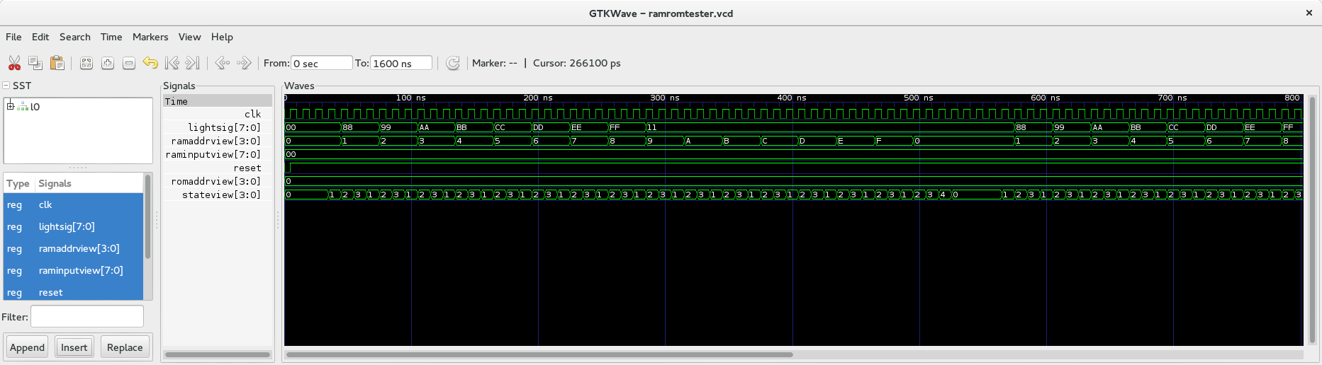
-
The second part of the state machine should read the contents of the
ROM and assign them to the RAM. This will also be be a multistep
process. You may be able to compress the process into fewer clock
cycles, but the following steps are a good way to start. Both
ROM_ADDR and RAM_ADDR should should be "0000" when the state machine
enters state 4 (0100). From the last state of the second half, if
ROM_ADDR is 0 (the circuit has wrapped around) then return to part one
where the circuit reads through the contents of the RAM.
step 1 (state 0100): assign the value on the ROM_WIRE to RAM_INPUT, increment ROM_ADDR, set write_enable to '1'. step 2 (state 0101): set write enable to '0' step 3 (state 0110): increment RAM_ADDR; if ROM_ADDR is 0, goto state 0000, else state 0100. You can use the same test file again to simulate the circuit. But this time, the second time the RAM is output it should have the contents of the ROM. Be sure to document your GHDL testing for your writeup.
- Add a slowclock to your circuit and demonstrate the circuit on the board.
- Make an interesting pattern in the ROM and RAM to make a light show.
Extensions
- See how few states you can use to execute this task. Be sure that the task is operating properly if you do this.
- Enable some kind of user input to the task.
- Write a Python program that can generate an MIF file from some other, more easily readable, format.
- Add a hold/freeze button to the state machine.
- Have the light output be the RAM output or the ROM output depending on the state.
Writeup
Create a wiki page with your writeup. For each task, write a short description of the task, in your own words.
- Include a description of your top-level design.
- Include the initial contents of both your RAM and ROM.
- Describe the GHDL/hardware testing you undertook to prove the circuit works. A short video is strongly recommended.
- Include a description, and pictures, of any extensions.
- Please supply a list of people you worked with, including TAs, and professors. Include in that list anyone whose code you may have seen, such as those of friends who have taken the course in a previous semester.
Handin
Give your wiki page the label cs232f16project6.
Put your VHDL files in your Private subdirectory on the handin server in folder for this project. If you have any issues with the server, use vpn.colby.edu or send a tgz or zip file to the prof.